Metalens technology represents a groundbreaking advancement in optical engineering, leveraging the power of metasurfaces to create miniaturized lenses that are reshaping consumer electronics. Unlike traditional lenses made of polished glass or plastic, metalenses can manipulate light using tiny structures, enabling new functionalities in devices while significantly reducing size and production costs. This innovative technology has seen widespread adoption, with millions of these light-focusing metasurfaces integrated into popular gadgets like smartphones and tablets. As the demand for compact and versatile optical solutions continues to rise, the application of metalens technology is becoming increasingly vital, from enhancing photography to improving 3D sensing capabilities. With its potential to disrupt conventional optics, metalens technology not only paves the way for cutting-edge polarized cameras but also opens the door to a myriad of applications across various sectors.
The exploration of metalens technology, often referred to as advanced lens-making through metasurfaces, is transforming the way we understand optical technology. These innovative mini-lenses are enabling manufacturers to break free from the constraints of traditional lens designs, unlocking new applications in varied consumer devices. With a focus on light manipulation at the nanoscale, this optical revolution offers unprecedented possibilities, from enhancing image capture in everyday electronics to pioneering new methods for depth sensing in augmented reality. As a result, the emergence of this novel lens technology serves as a catalyst for innovation, reshaping industries and providing a glimpse into the future of optics in consumer markets. Whether through novel polarization techniques or compact design features, the possibilities for this groundbreaking tech are vast and exciting.
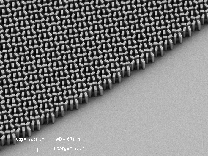
The Evolution of Metalens Technology
Metalens technology stands at the forefront of optical innovation, transforming how lenses are conceptualized and manufactured. Originating from research at Harvard University’s Capasso Lab, this cutting-edge technology utilizes metasurfaces—thin films of engineered materials with intricate nanostructures capable of bending light in unprecedented ways. This advancement has overturned the decades-old paradigm of relying on bulky, curved glass or plastic lenses. With the introduction of mini-lens designs, we are now witnessing a revolution in consumer electronics, where these tiny yet powerful devices can fit seamlessly into smartphones, tablets, and other gadgets, adapting to the compact needs of modern design.
As the application of metalens technology broadens, its impact extends beyond merely replacing traditional components; it paves the way for new functionalities within existing technologies. For instance, in devices like smartphones, the incorporation of these metasurfaces facilitates advanced imaging capabilities, such as depth perception and 3D mapping, which were previously restricted by bulky camera setups. The swift transition from the lab to mass production is a testament to the technology’s maturity and the pressing market demand for miniaturized optical solutions.
The Impact of Metasurfaces on Consumer Electronics
Metasurfaces have emerged as pivotal players in the consumer electronics sector, serving as the backbone of many modern devices. The ability to manufacture these light-focusing metasurfaces in semiconductor chip foundries has allowed companies like Metalenz to scale their production to meet increasing demands in the marketplace efficiently. Products equipped with these advanced lenses, such as the latest iPads and smartphones, are not only lighter and more compact but also offer enhanced performance. This is particularly crucial in a landscape where device makers continually seek thinner profiles without compromising on functionality.
Furthermore, the introduction of such technology contributes significantly to the competitive landscape among tech giants. By integrating metasurfaces, companies can improve camera quality and introduce features like facial recognition and augmented reality with lower production costs, thereby enhancing user experiences. The competitive edge provided by Metalenz’s products illustrates how advanced optical technologies can redefine the capabilities of consumer devices, creating smarter and more intuitive interactions for users.
Innovative Applications of Metalens in Optical Technology
While metalens technology is revolutionary in itself, its potential applications are even more exciting. Researchers and developers are envisioning uses beyond standard imaging. For instance, the concept of a polarization camera developed by Metalenz could provide substantial advancements in security and health monitoring. By leveraging polarization signatures unique to each individual, this technology can distinguish between genuine users and potential imposters, enhancing security protocols in smartphones and other devices.
Additionally, these polarization metasurfaces hold promise in medical fields, where the detection of anomalies in skin surfaces could lead to earlier diagnoses of conditions such as skin cancer. The ability to condense such complex functionalities into miniature modules opens avenues for creating multifunctional devices, integrating health monitoring and personal security into everyday electronics. This shift not only enhances the utility of consumer products but also emphasizes the versatility and significance of innovative optical technologies in our daily lives.
From Concept to Mass Production: The Metalenz Journey
The journey of Metalenz from a conceptual breakthrough in the lab to mass production is a remarkable story of innovation and collaboration. Driven by the initial research of Professor Federico Capasso and the subsequent contributions of Rob Devlin, Metalenz has successfully navigated the complexities of bringing groundbreaking technology into the marketplace. With the target of mass adoption, the startup has made strategic partnerships within the semiconductor industry, allowing for efficient production while maintaining high quality.
This proactive approach not only positions Metalenz as a leader in the optics space but also illustrates how academic research can fuel entrepreneurial ventures. The rapid transition from a prototype developed in 2016 to an operational company capable of producing millions of units annually underscores the importance of institutional support and the transformative potential of emerging technologies in reshaping industry standards.
Challenges and Opportunities in Optical Technology
In the realm of optical technology, challenges often abound, especially as industries race to stay ahead of competitors. Metalenz faces the ongoing challenge of maintaining its innovative edge in a rapidly evolving market where many entities are investing in similar advances. The constant pursuit of perfection in product development, coupled with manufacturing scaling, requires a diligent approach to sustain their lead in metasurface technology.
However, these challenges present vast opportunities for growth and innovation. As competitors seek to bridge the technological gap, Metalenz can leverage its existing market presence and consumer base to continuously introduce improved products. Developing new applications for existing metasurfaces, such as enhanced depth imaging and multi-functionality, presents exciting avenues for differentiation and expansion within the consumer electronics sector.
Future Innovations with Polarization Technology
The future of optical technology lies significantly in advancements associated with polarization. Metalenz are spearheading initiatives focused on the development of Polar ID, which utilizes light polarization to provide heightened security features. By crafting a much smaller and cost-effective polarization metasurface, the company can democratize this technology, making it accessible for widespread use in various consumer devices. This could lead to a new industry standard in how security measures are integrated into everyday electronics.
Moreover, the implications of polarization technology extend beyond security. Its potential applications in environmental monitoring, such as assessing air quality or detecting harmful substances, could significantly influence public health initiatives and safety protocols. The ongoing exploration of these innovative applications reflects the dynamic nature of optical technology and its capability to impact various sectors beyond traditional imaging.
Cross-disciplinary Collaborations Driving Innovation
The success story of Metalenz is a testament to the power of cross-disciplinary collaboration in fostering innovation. By merging expertise from diverse fields—including physics, engineering, and material science—the team has cultivated an environment ripe for creativity and groundbreaking discoveries. This synergy is evident in how Metalenz was able to transition from a university research project to a successful startup producing millions of units for the consumer electronics market.
Such collaborations not only enhance the technical capabilities of a team but also drive fresh ideas and approaches to problem-solving. The interaction between academic researchers and industry professionals allows for the rapid translation of theoretical discoveries into practical applications. Metalenz exemplifies how fostering diverse perspectives leads to extraordinary advancements and products that can redefine industries and consumer experiences.
The Role of Consumer Demand in Shaping Technology
Consumer demand plays a pivotal role in shaping the trajectory of technological advancements, particularly in the field of optics. The widespread adoption of devices featuring metalens technology indicates a significant shift towards compact, efficient solutions in the consumer electronics marketplace. As users increasingly seek enhanced features without the burden of size and weight, companies are compelled to innovate rapidly to meet these expectations.
With consumers being more tech-savvy and discerning, their preferences significantly influence manufacturers’ strategies. This demand not only fuels the need for better imaging technology but also encourages companies like Metalenz to explore creative applications of metasurfaces. The rising interest in devices that incorporate advanced capabilities while maintaining affordability continually drives progress in optical technology.
Metalenz’s Vision for Sustainable Technology
Looking ahead, Metalenz envisions their technology contributing to a more sustainable future. The shift towards smaller, more efficient optical components aligns with global sustainability goals in electronics manufacturing. By reducing the size and cost of essential components, the startup advances the design of greener devices that utilize fewer resources and energy.
Moreover, as electronics recycling becomes more critical, Metalenz’s smaller products can facilitate easier disassembly and recycling processes. By prioritizing sustainability in design and production, Metalenz is contributing to a circular economy model, ensuring that their innovations not only meet current consumer demands but also align with broader environmental considerations. This forward-thinking approach positions the company as a leader in not just technological advancement but also ecological responsibility.
Frequently Asked Questions
What is metalens technology and how does it differ from traditional lens systems?
Metalens technology utilizes metasurfaces composed of nano-scale structures to manipulate light, offering a thinner and lighter alternative to traditional lens systems that rely on curved glass. This innovation allows for more compact designs in consumer electronics, improving device performance while reducing bulk.
How are metalenses used in consumer electronics?
Metalenses are integrated into various consumer electronics, such as smartphones, tablets, and cameras, to enhance optical functionalities like focusing and depth sensing. They enable high-performance imaging capabilities without the size constraints of conventional lenses.
What are the benefits of using metasurfaces in optical technology?
Metasurfaces offer numerous advantages in optical technology, including reduced weight and size, lower production costs, and the ability to mass-produce using semiconductor manufacturing techniques. This facilitates the integration of advanced optical functionalities into a wide range of consumer devices.
How does Metalenz’s mini-lens technology contribute to advancements in optical imaging?
Metalenz’s mini-lens technology revolutionizes optical imaging by enabling thinner, lighter lenses with improved performance. By applying principles of metalens technology, devices can achieve better focusing capabilities and enhanced depth perception while minimizing space requirements.
What role do polarization cameras play in metalens technology?
Polarization cameras enhance the functionality of metalenses by capturing light polarization information, which can be crucial for applications like facial recognition and environmental monitoring. Metalenz’s innovations aim to make these cameras smaller and more affordable, broadening their accessibility.
How is Metalenz aiming to innovate beyond traditional metalens applications?
Metalenz is focused on developing new functionalities through its technology, such as Polar ID, which utilizes light polarization for security applications. These innovations are designed to enhance consumer electronics while maintaining a low cost and compact size.
What potential does metalens technology have for the future of optical devices?
The future of optical devices is promising with metalens technology, as it enables the development of smaller and more efficient imaging solutions. This technology not only enhances current capabilities but also opens up new possibilities in areas like augmented reality, advanced sensing, and medical diagnostics.
Why are metasurfaces considered a breakthrough in optical technology?
Metasurfaces are considered a breakthrough because they fundamentally change how light is manipulated compared to conventional optics. They allow for unprecedented control over light behavior at the nanoscale, paving the way for new applications in consumer electronics and beyond.
| Key Points |
|---|
| Rob Devlin developed a new type of mini-lens during his Ph.D. at Harvard, focusing on metasurfaces that bend light. |
| Metalenz, founded in 2016, has produced around 100 million metasurfaces for consumer electronics, integrating them into popular devices like iPads and Samsung phones. |
| The company focuses on disrupting conventional optics with innovative fabrication methods, paving the way for mass production. |
| Metalenz collaborates with companies like STMicroelectronics for applications in 3D sensing, facial recognition, and augmented reality. |
| Future projects include Polar ID technology, which utilizes polarization for added security in smartphones at a significantly reduced cost. |
| Metalenz continues to innovate while facing competition from other companies trying to develop similar technologies. |
Summary
Metalens technology represents a groundbreaking advancement in optical engineering, transforming how we perceive and manipulate light. Originating from research at Harvard, this innovative mini-lens technology enables smaller, cheaper, and highly efficient lenses, which have already been integrated into a variety of consumer electronics. With the ongoing development of applications such as Polar ID for enhanced security and accurate measurements, the future of metalens technology looks promising. As more industries adopt this cutting-edge solution, the potential for new functionalities and improvements in existing products will continue to revolutionize the tech landscape.